3.8mm 10layer Counterbore Hole 6.0mm Depth 1.5mm Multilayer Complex Circuit Board PCB
Package Size 1.00cm * 1.00cm * 1.00cm Package Gross Weight 1.000kg Company Profile welcome to visit gawinpcba.en.made-in
Description
Basic Info.
| Model NO. | GW-1920422794 |
| Application | Communication |
| Flame Retardant Properties | V0 |
| Processing Technology | Enig |
| Production Process | Additive Process |
| Base Material | Copper |
| Insulation Materials | Epoxy Resin |
| Brand | 1 |
| Board Thickness | up to 8mm |
| Counterbore Hole | 6.0mm |
| Cu Thickness | up to 12oz |
| Layer Count | up to 64 |
| Transport Package | Vacuum + Carton Packing |
| Specification | 1 |
| Trademark | 1 |
| Origin | Made in China |
| HS Code | 8534001000 |
| Production Capacity | 500000PCS/Month |
Packaging & Delivery
Package Size 1.00cm * 1.00cm * 1.00cm Package Gross Weight 1.000kgProduct Description
Company Profile welcome to visit gawinpcba.en.made-in-china.comShanghai Gawin Electronic Technology Company, a specialized PCB manufacturer with one-stop service from PCB design to PCB manufacture to BOM components procurement to PCB Assembly toFinished Product testing.
Ability Show
PCB Layout
Our dedicated team provides high quality PCB design service for more than 5,000 customers, such as Intel, Cisco, Huawei, Freescale, TI, Lenovo, etc. in the past 15 years. We have 50+ PCB designers located in our offices in Shenzhen, Beijing, Shanghai, doing PCB layout for customers from all over the world. We constantly strive to further our technological capabilities, and are now working on DDR4 and 25Gbps+ backplane signal design and simulation.I Advantages
1. Experienced experts providing high quality work;
2. Large team with excellent customer service;
3. Independently developed software to enhance design efficiency;
4. Keep up-to-date with technology;
II PCB Layout Business Model
1. PCB Design Total Solution: PCB footprint creation, Netlist import, Placement, Routing, QA & Review,DFM checking, Gerber out;
2. On-site Service: work together with your engineers in your office;
3. Consulting and Training: provide consulting and training services of PCB design;
Physical Parameters
Highest layers::42 Layers
Maximum PIN count:69000+
Maximum connections:55000+
Minimum line width:2.4mil
Minimum line spacing:2.4mil
Minimum via:6mil(4mil laser hole)
Maximum BGA in a single PCB:62
Maximum BGA PIN spacing:0.4mm
Maximum BGA PIN count:2597
Highest speed signal:10G CML
Involved Chipset Scheme
Network processor series:IXP2400 IXP2804 IXP2850…
Intel Sandy Bridge series:Intel Core i7 Extreme Core i5…
Intel XEON server series:Xeon® E7 Family® 5000 Sequence…
Marvell series:MX630 FX930 FX950…
Broadcom Sonet/SDH series:BCM8228 BCM8105 BCM8129…
Broadcom Gigabit Ethernet switch series:BCM5696 BCM56601 BCM56800…
QUALCOMM/Spreadtrum/MTK platform:QSC60xx SC88xx SC68xx Mt622x…
Freescale PowerPC series:MPC8541 MPC8548 MPC8555 MPC8641…
FPGA DSP series of chips:Virtex-7 Spartan-6 TMS320C5X…Backplane, High-Speed PCB design, A/D PCB design, HDI/ALIVH/Buried resister/Buried capacitance,
Flex PCB/Rigid-Flex Board, ATE ;
High Speed and High density PCB Design for IT Communication, Computer, Medical, Digital and consumer
PCB Main Capabilities:
Layer Count: 2L~64L
Max.Board Thickness: 10mm
Min. Trace Width/Space: Inner 2.5/2.5mil, Outer 3/3mil
Trace Width/Spacing Tolerance:±20%; ±10% for signal trace areas by special control
Max. Copper Weight: 12oz (Inner/Outer Layer)
Min. Drilling Size: Mechanical 0.15mm, Laser 0.1mm
Max. Unit PCB Size: 800mmX520mm
Max. Delivery Panel Size: 1200mm×570mm
Max. Aspect Ratio: 18:1
Surface Finish: LF-HASL, ENIG, Imm-Ag, Imm-Sn, OSP, ENEPIG, Gold Finger etc.
Impedance Tolerance: ±8%Special Materials:
1, Lead-free/Halogen-free:
EM827, 370HR, S1000-2, IT180A, EM825, IT158, S1000 / S1155, R1566W, EM285, TU862HF;
2, High Speed: Megtron6, Megtron4,Megtron7,TU872SLK,FR408HR,N4000-13 Series,MW4000,MW2000,TU933;
3, High Frequency: Ro3003, Ro3006, Ro4350B,Ro4360G2, Ro4835, CLTE, Genclad, RF35, FastRise27;
4, FPC Materials: Polyimide, Tk, LCP, BT, C-ply,Fradflex, Omega , ZBC2000.
High Layer Count PCBs
High layer count PCBs, widely found in file servers, data storage, GPS technology, satellite systems, weather analysis and medical equipment are usually ≥12L with special performance requirement raw material.
FPC Main Capabilities:
Single side/Double side, Multilayer(6 layers or below)
Roll to Roll manufacturing, enable the ability of handling thin base material
0.035mm small via
0.035/0.035mm trace width/space design
From SMT to adhesive dispensing, ICT to FCT, assembly & Test full process capability, One-stop shop service for our customers
5G FPC Simulation/Manufacturing/Test One-stop shop service
Flex-rigid PCB Main Capabilities
Standard Panel Size: 500x600mm
Copper Thickness: 6 OZ
Final Thickness: 0.06-6.0mm
Layer Count: Up to 20L
Material: PI, PET, PEN, FR4, PI
Min Line Width/Spacing: 3/3mil
Min Drill Hole Size: 6mil
Min Via Size: 4mil (Laser)
Min Micro Via Size: 4mil (Laser)
Min Slot Size: 24milx35mil(0.6x0.9mm)
Min Hole Ring:
Inner 1/2OZ 4mil (0.10 mm)
Inner 1OZ 5mil (0.13 mm)
Inner 2OZ 7mil (0.18mm)
Outer 1/3-1/2OZ 5mil (0.13 mm)
Outer 1OZ 5mil (0.13 mm)
Outer 1OZ 8mil (0.20mm)
Stiffener:
Stiffener Material Polyimide/FR4
PI Stiffener Registration 10mil (0.25mm)
PI Stiffener Tolerance 10%
FR4 Stiffener Registration 10mil (0.25mm)
FR4 Stiffener Tolerance 10%
Coverlay Color White, Black, Yellow, Transparent
Surface Finish:
ENIG Ni: 100-200μ'', Au: 1-4μ''
OSP 8-20μ''
Immersion Silver Silver: 6-12μ''
Gold Plating Ni: 100-200μ'', Au: 1-15μ''
Outline Tolerance of Punch:
Precision Mould +/-3mil (0.08 mm)
Ordinary Mould +/-4mil (0.10 mm)
Knife Mould +/-9mil (0.23 mm)
Hand Cutting +/-16mil (0.41 mm)
Electrical Test Voltage: 50-300V
Metal Base PCBs Capabilities:
Max. Layer: 1-10 layers
Max. Board Thickness: 4.0mm
Max. Delivery Panel Size: 740mm x 540mm
Max. Copper Weight: 6oz (Inner/Outer Layer)
Drilling Size on Aluminum Base: Max. 6.4mm, Min. 0.55mm
Drilling Size on Copper Base: Max. 6.0mm, Min. 0.6mm
Max. Breakdown Voltage: 6000V/AC
Heat Dissipation Performance: 12W/m.K
Metal Base Material Type: Copper/Aluminum/Stainless Steel/Iron
Metal Base Printed Circuit Board
MPCB, a metal-based PCB, is comprised of a metal substrate (ie Aluminum, Copper or Stainless Steel ect.,), thermal dissipating dielectric and the copper circuit. Due to its superior heat dissipation, MPCBs are used for a wide array of applications. You can find them in power supplies, LED lighting or anywhere that heat is a major factor.
HDI High Density Interconnect PCB Main Capabilities
HDI Layer Count: 4L-32L mass production, 34L-64L quick-turn
Material: High Tg material (Recommend Shengyi Material)
Finished Board Thickness: 0.8-4.8mm
Finished Copper Thickness: Hoz-8oz
Max. Board Size: 600X800mm
Min. Drilling Size: 0.15mm, 0.1mm(laser drilling)
Blind/Buried vias depth ratio: 1:1
Min. Line Width/Space inner: 2/2mil, outer 3/3mil
Surface Finish: ENIG, Immersiong Silver, Immersion Sn, Plated Gold, Plated Sn, OSP ect.
Standard: IPC Class 2, IPC Class 3, Millitary
Application: Industrial, Automotive, Consumer, Telecom, Medical, Military, Security ect.
Blind&Buried Structure: 3+N+3 to any layer
Mass SMT Main Capabilities
Layer Count: 1Layer - 30Layer PCB
Max PCB size: 510x460mm
Min. PCB size: 50x50mm
Board thickness: 0.2-6mm
Min. Components size: 0201-150mm
Max. Components size: 25mm
Min. lead pitch: 0.3mm
Min. BGA ball pitch: 0.3mm
Placement precision: +/-0.03mm
Other: Laser cut for Stencil manufacture for manual, semi-automatic and fully automatic solder print machine, the accuracy can be 5um.
Top Advantages:1, The first to introduce aerospace system quality control standard.
2, No limit to MOQ, meet different customer demands by all means.
3, Speedy delivery! Punctual, Fast! Make sample in 24h, small and medium volume production for 3-5 days,mass production for 9-12 days.
4, Preferred SMT factory in Science Park with public praise of high quality and customer loyalty over ten years.
5, Take charge of PCB production, SMT processing, procurement of compo-nents, tests and general assembly.
6, Long-term partners cover Lenovo,HUAWEI, China Mobile and some military units.
7, Reduce cost for you! Excellent and speedy one-stop manufacturing service will save time, trouble and money for you.
8, Sophisticated SMD mydata and accurate AOI are tailor-made for high-end products.
9, Through 36 test procedures of TUV, product percent of pass is 99.97%.
10, Strong senior engineering team will build a firewall of quality problems.
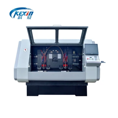
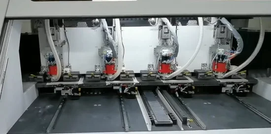
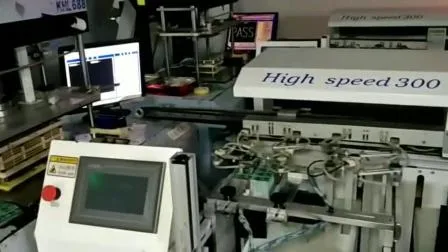
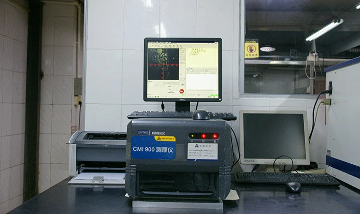
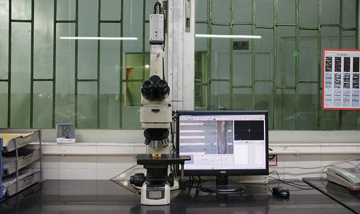
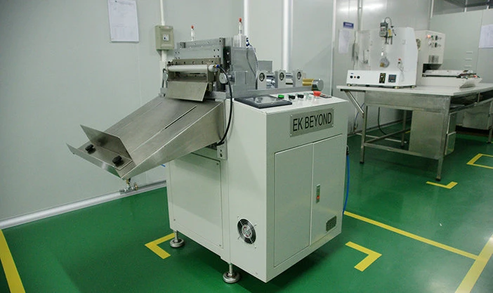
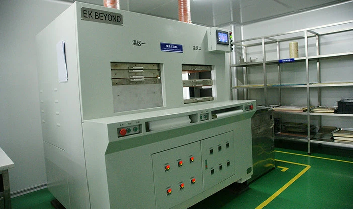
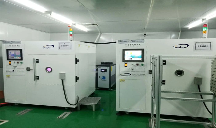
Main Equipement Show
Prev: Advanced Multilayer Flex
Next: High Quality Multi
Our Contact
Send now